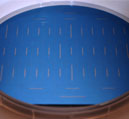
The Microfabrication and Microfluidics Unit of the BEPS Shared Resource specializes in the following:
- Design, fabrication, and implementation of microfluidic devices
- Rapid turnaround of single or multi-layer templates with lateral dimensions down to ~1.5 µm
- Microfabricated devices made from silicon/glass, PDMS, thermoplastics, and agarose.
- Structured surface modification, including microcontact printing
- Developing in vitro platforms that model tissue environments for realistic studies of cellular interactions. Methods include microfabrication, hydrogel fabrication and characterization, 3D printing, electrospinning, and finite element modeling
Our goal is close collaboration and rapid, iterative design. Although our preferred mode of operation is to disseminate microfabrication technology by having researchers from other laboratories participate actively in device fabrication, we can make templates and devices if desired.
We are located in Building 13 on the NIH campus.


The Microfabrication and Microfluidics Unit has the following capabilities on-campus
- Contact aligner for wafers up to 4” diameter, lateral resolution down to 1.5 µm.
- Software for photomask design.
- Spin-coater for rigid and flexible substrates
- Protocols for fabrication of
- SU-8 templates with heights from 1µm to 250µm
- Dry-film resist templates on flexible substrates
- PDMS and agarose devices
- Paper microfluidic devices
- Plasma cleaner (air or oxygen) for activating polymer surfaces
- Contact angle measurement
- Extrusion bioprinter with temperature-controlled stage
- Rheometer for viscoelastic characterization of hydrogels
- Capability for hot embossing thermoplastics
- Thermal evaporator for metal (Cr/Au, Al) deposition
- Expertise in implementing flow control (displacement, electokinetic, and pressure) for microfluidic devices
For silicon/glass devices, tight-tolerance features, or high-yield requirements we can use facilities at NIST.

